ATmega328P
2018-01-27 (updated 2018-02-19)The ATmega328P is an 8-bit AVR microcontroller (summary/datasheet). It's the "picoPower®" variant of the ATmega328, and the two are largely similar. It used to be made by Atmel, but Atmel was recently taken over by Microchip (the makers of the PIC line).
Other chips in the same family include the ATmega48, ATmega88, and ATmega168. They're basically the same chip, but with different amounts of flash ROM, RAM, and EEPROM space. The digits before the final 8 say how much flash ROM the chip has (in kB). The ATmega8 is a close cousin.
Pinout (28-pin PDIP)
Most pins serve multiple purposes, so I've broken them out by category. See the Arduino pin mapping (or below) for a comprehensive summary.
Power
1 2 3 4 5 6 7 8 9 10 11 12 13 14 15 16 | +-----------+
RESET -| 1 \_/ 28 |-
-| 2 27 |-
-| 3 26 |-
-| 4 25 |-
-| 5 24 |-
-| 6 23 |-
VCC -|* 7 22@|- GND
GND -|@ 8 21 |-
-| 9 20*|- AVCC
-| 10 19 |-
-| 11 18 |-
-| 12 17 |-
-| 13 16 |-
-| 14 15 |-
+-----------+
|
Clock
1 2 3 4 5 6 7 8 9 10 11 12 13 14 15 16 | +-----------+
-| 1 \_/ 28 |-
-| 2 27 |-
-| 3 26 |-
-| 4 25 |-
-| 5 24 |-
-| 6 23 |-
-|* 7 22@|-
-|@ 8 21 |-
XTAL1, TOSC1 -| 9 20*|-
XTAL2, TOSC2 -| 10 19 |-
-| 11 18 |-
-| 12 17 |-
-| 13 16 |-
CLKO -| 14 15 |-
+-----------+
|
Digital ports
There are 3 ports (B, C, D) with 8 pins each (not contiguous!), except there's no pin C7.
Pin C6 is special, since it's shared with RESET; it can only be used when RSTDISBL is programmed.
1 2 3 4 5 6 7 8 9 10 11 12 13 14 15 16 | +-----------+
C { C6 -| 1 \_/ 28 |- C5 \
/ D0 -| 2 27 |- C4 |
| D1 -| 3 26 |- C3 |
D | D2 -| 4 25 |- C2 | C
| D3 -| 5 24 |- C1 |
\ D4 -| 6 23 |- C0 /
-|* 7 22@|-
-|@ 8 21 |-
B / B6 -| 9 20*|-
\ B7 -| 10 19 |- B5 \
/ D5 -| 11 18 |- B4 |
D | D6 -| 12 17 |- B3 | B
\ D7 -| 13 16 |- B2 |
B { B0 -| 14 15 |- B1 /
+-----------+
|
Pin change interrupts
The 3 ports (B, C, D) correspond directly to the pin change mask registers (PCMSK0, PCMSK1, PCMSK2).
Hence, there's no PCINT15.
1 2 3 4 5 6 7 8 9 10 11 12 13 14 15 16 | +-----------+
1 { PCINT14 -| 1 \_/ 28 |- PCINT13 \
/ PCINT16 -| 2 27 |- PCINT12 |
| PCINT17 -| 3 26 |- PCINT11 |
2 | PCINT18 -| 4 25 |- PCINT10 | 1
| PCINT19 -| 5 24 |- PCINT9 |
\ PCINT20 -| 6 23 |- PCINT8 /
-|* 7 22@|-
-|@ 8 21 |-
0 / PCINT6 -| 9 20*|-
\ PCINT7 -| 10 19 |- PCINT5 \
/ PCINT21 -| 11 18 |- PCINT4 |
2 | PCINT22 -| 12 17 |- PCINT3 | 0
\ PCINT23 -| 13 16 |- PCINT2 |
0 { PCINT0 -| 14 15 |- PCINT1 /
+-----------+
|
External interrupts
1 2 3 4 5 6 7 8 9 10 11 12 13 14 15 16 | +-----------+
-| 1 \_/ 28 |-
-| 2 27 |-
-| 3 26 |-
INT0 -| 4 25 |-
INT1 -| 5 24 |-
-| 6 23 |-
-|* 7 22@|-
-|@ 8 21 |-
-| 9 20*|-
-| 10 19 |-
-| 11 18 |-
-| 12 17 |-
-| 13 16 |-
-| 14 15 |-
+-----------+
|
Timers
1 2 3 4 5 6 7 8 9 10 11 12 13 14 15 16 | +-----------+
-| 1 \_/ 28 |-
-| 2 27 |-
-| 3 26 |-
-| 4 25 |-
OC2B -| 5 24 |-
T0 -| 6 23 |-
-|* 7 22@|-
-|@ 8 21 |-
-| 9 20*|-
-| 10 19 |-
T1, OC0B -| 11 18 |-
OC0A -| 12 17 |- OC2A
-| 13 16 |- OC1B
ICP1 -| 14 15 |- OC1A
+-----------+
|
Analog
ADC6 and ADC7 are only present in the 32-pin packages.
1 2 3 4 5 6 7 8 9 10 11 12 13 14 15 16 | +-----------+
-| 1 \_/ 28 |- ADC5
-| 2 27 |- ADC4
-| 3 26 |- ADC3
-| 4 25 |- ADC2
-| 5 24 |- ADC1
-| 6 23 |- ADC0
-|* 7 22@|-
-|@ 8 21 |- AREF
-| 9 20*|-
-| 10 19 |-
-| 11 18 |-
AIN0 -| 12 17 |-
AIN1 -| 13 16 |-
-| 14 15 |-
+-----------+
|
USART, I2C, SPI
1 2 3 4 5 6 7 8 9 10 11 12 13 14 15 16 | +-----------+
-| 1 \_/ 28 |- SCL0 \
/ RXD0 -| 2 27 |- SDA0 / I2C
| TXD0 -| 3 26 |-
USART . -| 4 25 |-
. -| 5 24 |-
\ XCK0 -| 6 23 |-
-|* 7 22@|-
-|@ 8 21 |-
-| 9 20*|-
-| 10 19 |- SCK0 \
-| 11 18 |- MISO0 | SPI
-| 12 17 |- MOSI0 |
-| 13 16 |- SS0 /
-| 14 15 |-
+-----------+
|
Minimal hookup
At the very least, VCC and GND must be supplied, with 1.8 V to 5.5 V between them.
It's good practice to connect the two GND pins together, but it's not absolutely necessary (i.e. you should do it on a PCB, but your circuit will probably work without it when prototyping).
The datasheet advises connecting AVCC to VCC when not using the ADC, but this is also not absolutely necessary.
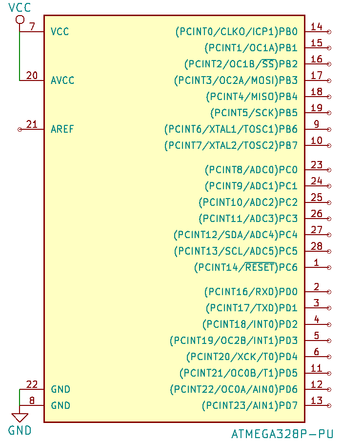
If you're running from an internal oscillator, that's all you need to have the chip going. Keep in mind that the maximum clock speed is limited by the supply voltage.
Compiling
On Arch Linux, the avr-gcc, avr-libc, and avr-binutils packages are needed.
Here's a minimal blinking program:
1 2 3 4 5 6 7 8 9 10 11 12 13 14 15 16 17 18 19 20 | #include <avr/io.h>
#include <avr/wdt.h>
#include <util/delay.h>
int main(void) {
// Clear reset flags.
MCUSR = 0;
// Set pin D5 to output.
DDRD |= _BV(5);
for (;;) {
// Toggle pin D5.
PORTD ^= _BV(5);
// Wait 500 ms.
_delay_ms(500);
}
return 0;
}
|
Build an ELF using
1 | avr-gcc -Os -mmcu=atmega328p -DF_CPU=1000000 -o main.bin main.c
|
This assumes that your clock is at 1 MHz, which is true for a brand new chip with original fuse settings.
Otherwise, set F_CPU accordingly.
It also optimizes for size, which is often what you want for a microcontroller.
If you just want to compile an object file and not link it, use -c as usual.
You can take a look at the result with
1 | avr-objdump -D main.bin
|
To make an Intel HEX file, use
1 | avr-objcopy -j .text -j .data -O ihex main.bin main.hex
|
Programming
On Arch Linux, the avrdude package gives you avrdude.
You may want to automatically set the permissions of your programmer device to something permissible.
For example, for a USBtinyISP-derived programmer like the SparkFun Pocket AVR Programmer, you could make the file /etc/udev/rules.d/98-usbtiny.rules with the contents
1 | ATTRS{idVendor}=="1781", ATTRS{idProduct}=="0c9f", MODE="0666"
|
To see a list of programmers supported by avrdude, run
1 | avrdude -c '?'
|
I'm assuming usbtiny in the following, because that's what I use.
To see information about the current device (and make sure everything is set up correctly), use
1 | avrdude -c usbtiny -p atmega328p -vvv
|
It should output (among other things)
1 | avrdude: Device signature = 0x1e950f (probably m328p)
|
To flash an Intel HEX file (in this case main.hex), use
1 | avrdude -c usbtiny -p atmega328p -U flash:w:main.hex:i
|
This means "write the Intel HEX file main.hex to the flash ROM".
Fuses
Some aspects of the chip's operation (e.g. the clock source) can only be changed by setting "fuses". The fuse values can only be modified when the chip is being programmed. For whatever reason, the fuse logic is inverted, so programming a bit means setting it to 0, not 1!
The ATmega328P has 3 fuse bytes:
1 2 3 4 5 6 7 8 9 10 11 12 | Extended High Low
+-------- RSTDISBL +-------- CKDIV8
|+------- DWEN |+------- CKOUT
||+------ SPIEN ||+------ SUT1 \
|||+----- WDTON |||+----- SUT0 /
11111 ||||+---- EESAVE ||||+---- CKSEL3 \
|||||+--- BODLEVEL2 \ |||||+--- BOOTSZ1 \ |||||+--- CKSEL2 |
||||||+-- BODLEVEL1 | ||||||+-- BOOTSZ0 / ||||||+-- CKSEL1 |
|||||||+- BODLEVEL0 / |||||||+- BOOTRST |||||||+- CKSEL0 /
|||||||| |||||||| ||||||||
76543210 76543210 76543210
|
The factory defaults are
1 2 3 | E 0xff H 0xd9 L 0x62
11111111 11011001 01100010
76543210 76543210 76543210
|
This results in the following settings:
| Setting | Bits | Value |
|---|---|---|
CKSEL |
0010 |
Internal RC oscillator (8 MHz) |
SUT |
10 |
Maximum startup time |
CKOUT |
1 |
Pin 14 not used for clock output |
CKDIV8 |
0 |
Clock divided by 8 |
BOOTRST |
1 |
Application reset (no boot loader) |
BOOTSZ |
00 |
Maximum boot loader size |
EESAVE |
1 |
EEPROM erased on chip erase |
WDTON |
1 |
Watchdog forced reset disabled |
SPIEN |
0 |
Serial programming enabled |
DWEN |
1 |
debugWIRE disabled |
RSTDISBL |
1 |
Pin 1 used for reset |
BODLEVEL |
111 |
BOD disabled |
To get the full 8 MHz from the internal oscillator, unset CKDIV8 by programming 0xe2 to the low byte:
1 | avrdude -c usbtiny -p atmega328p -vvv -U lfuse:w:0xe2:m
|
The Engbedded AVR fuse calculator makes life a lot easier when changing fuses.
Target board
You need some way of connecting your programmer to your chip. The easiest way is to use a target board (make sure to get one with a ZIF socket!).
It's also straightforward to make a target board. If your programmer uses the standard AVR ISP header and cable, you can refer to the standard pinouts:
1 2 3 4 5 6 7 | +------+
+-----+ MOSI | 1 2 | VCC
MISO | 1 2 | VCC | 3 4 | GND
SCK 3 4 | MOSI RESET 5 6 | GND
RESET | 5 6 | GND SCK | 7 8 | GND
+-----+ MISO | 9 10 | GND
+------+
|
Here's how you might connect a header to the right spots beside the chip using jumper wires:
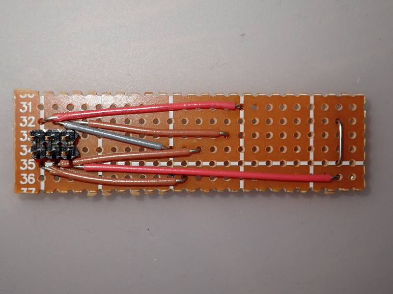
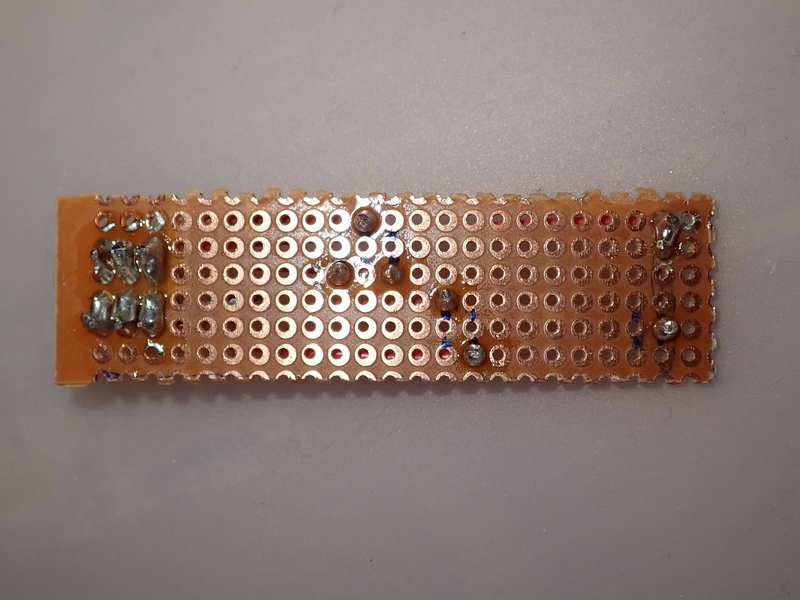 It would be better to use a shrouded header, but I didn't have any.
Then just add a ZIF socket and some female headers:
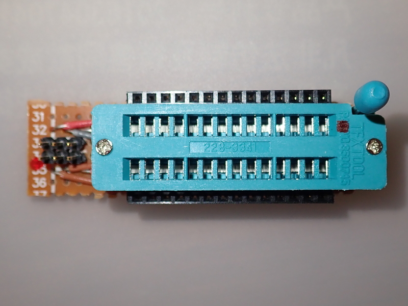
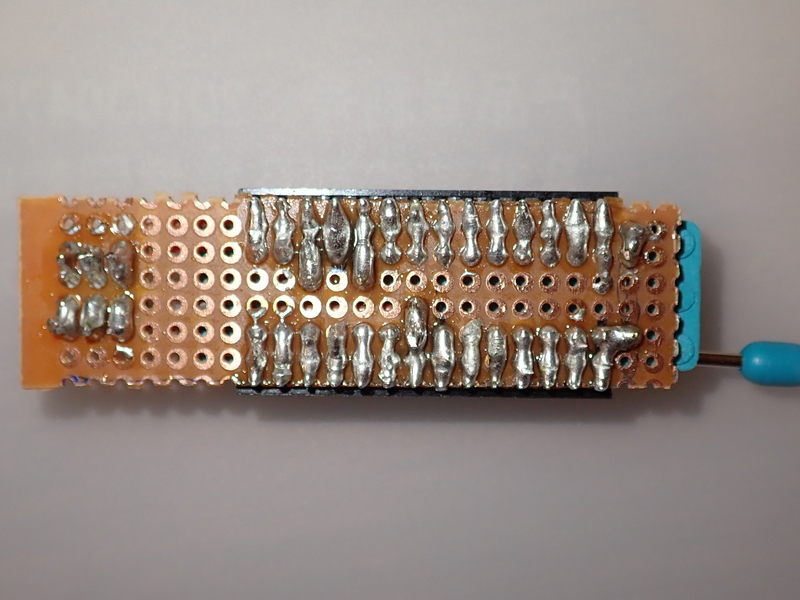 The red dots on the socket and ISP header indicate pin 1.
And here's how it looks all wired up and ready to go:
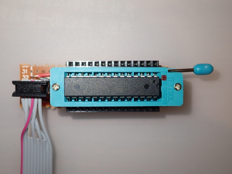
Fun fact: Just like a breadboard, this target board has enough parasitic capacitance that you can throw on a crystal without any load capacitors. As far as I can resolve with my scope, I get within 0.2% of the rated frequency with a 16 MHz crystal.
External clock
If you set CKSEL to 0000, the chip expects a ready-made clock signal on pin 9 (XTAL1).
You can do basically whatever you want here, like a 555 timer at 70 kHz.
Even if the chip is trying to use an external crystal on XTAL1 and XTAL2 (CKSEL set to one of the many crystal oscillator settings), you can feed it a square wave on XTAL1 and it will still work!
This is useful for rescue to switch back to the internal oscillator.
Just note that programming has to happen no faster than 4 times slower than the clock speed, so you might need to do something like
1 | avrdude ... -B 15kHz
|
Two-wire (I2C)
Pin 27 is SDA and pin 28 is SCL.
While there is hardware support for I2C, you'll need a library to use it if you don't want to mess around with the registers directly.
For a master device, you can use Peter Fleury's I2C Master Interface library.
It's GPLv3, and dead simple to use.
If your slave devices don't have pull-ups, you'll need 4.7 kΩ on both SCL and SDA.
The only files you need are i2cmaster.h and twimaster.c, which I'll assume are in i2cmaster/.
Build with -Ii2cmaster and include i2cmaster/twimaster.o when linking.
Set SCL_CLOCK to what you want to run the bus at, but be careful that your CPU clock speed allows for the setting.
Datasheet problems
The ATmega328/P - Complete Datasheet (Rev. B – 11/2016, dated "12/10/2016" and marked "Atmel-42735B-ATmega328/P_Datasheet_Complete-11/2016" on the bottom of each page) has some issues:
- "Table 6-1. PORT Function Multiplexing" has
PC[0]as pin 13 instead of 23. - "17.2.7. Pin Change Mask Register 1" talks about
PCINT[15:8], but there is noPCINT15.